|
|
|
|
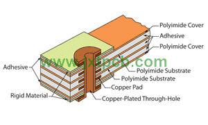
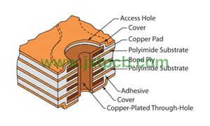
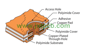
Double layer fpcb |
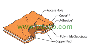
Single sided fpcb |
|
|
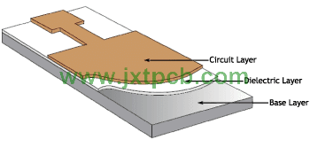
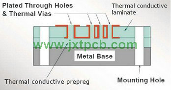
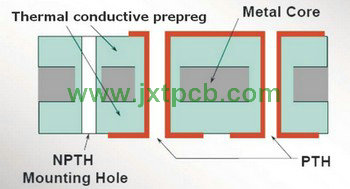
2 layer metal base pcb |
|
|
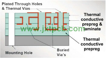
4 layer metal base pcb |
|
Via in pads |
HDI pcb / Buried and blind via pcb |
|
Heavy copper pcb / thicker copper pcb |
|
Jxtpcb is a full-service turnkey PCB solution that can handle everything from prototype to fabrication to assembly. We have been fabricating high quality standard PCB for over ten years and are fully compliant with ISO9001:2008 quality standards. All of our standard PCBs are IPC2 compliant, and we do strict internal quality assurance testing to ensure the board that arrives at your facility is one you know you can rely on.
We offer PCB solutions that fit your budget. You can order just a few prototype boards to test your design, and then place a bulk order for your standard PCBs to save even more money. We’ll give you a free instant quote so you’ll know just want to expect and so that you can plan accordingly. We also offer complete technical support from PCB experts. Call us up, chat online or email us with any questions, whichever is the most convenient for you. We’ll handle your concerns or questions as quickly as possible. We have obtained over 99 percent customer satisfaction rate, and as soon as you start ordering printed circuit boards from Jxtpcb, you’ll find out why.
1. Layers: 2-40 layers
2. Max manufacturing size: 700 mm*1500 mm
3. Copper foil thickness: 0.3 OZ- 20 OZ
4. Board thickness: 0.15 - 10 mm
5. Min Line Width/Space: 2.0 mil / 2.0 mil
6. Min finished holes size: 4 mil
7. Aspect ratio: 15 : 1
8. Surface treatment: lead free HASL, Immersion Gold,ENEPIG,Immersion Tin, Immersion Silver, Gold plating, OSP etc.
9. Fastest delivery time: 12-72 hours
10.Other Techniques:
Gold fingers, Blind via and Buried via holes,
Peelable solder mask, Carbon Mask,
Edge plating, Kapton tape,
Countersink/counterbore hole, Half-cut/Castellated hole,
Via tented/covered with resin, Via plugged/filled with resin,
Via in pad, Electrical Test,
Back drill, Press fit hole


