


Product Catalog
Contact us
Tel:86-755-29760917
Fax:86-755-23283744
Mobile:86-18927410165
Skype:jxtsales1 jxtpcb02
Msn:jxtchina@hotmail.com
Email:sales@jxtpcb.com
Whatsapp / Wechat : 86-18927410165
Fax:86-755-23283744
Mobile:86-18927410165
Skype:jxtsales1 jxtpcb02
Msn:jxtchina@hotmail.com
Email:sales@jxtpcb.com
Whatsapp / Wechat : 86-18927410165
![]()
![]()


Product Description
Jxtpcb progressive team of engineers, designers & support professionals have over 15 to 20 years of combined experience & are capable of handling the toughest design challenges in the industry.
Capabilities
- Digital & Analog, Mixed Signal
- Power Supply, Backplanes
- S/S, D/S & Multi-layers Rigid PCB
- Thru-Holes, SMT/BGA HIGH Density (Double Side Placement)
- Controlled Impedance
- Blind/Buried Vias
- High Speed Audio & Video
- Flex & Rigid Flex PCB
Services
- Schematic Capture & Modifications or Convert hand drawn
- Net-list Translation / Output
- PCB Layout – Rigid, Flex & Rigid Flex
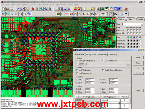
- Interactive / Auto Routing as per customer request
- Plotting Services
- CAD Files Translation / CAD software Training & Support available
- Gerber Files Panel optimize for cost effectiveness
Deliverables offered
- Output from Electronic Schematic capture in OrCAD V10-V16.2
- Bill of materials
- Circuit board foil layers, solder mask layers, overlay screening layers
- Fabrication drawing, assembly drawings, fabrication panel drawings
- SMT stencil artwork, CAM X-Y data file from FAB Master
- PDF file with all drawings for electronic documentation
- Gerber files, text & Excel files where applicable
- Native Board files from the latest versions of Mentor's PAD's, Cadence's OrCAD Layout and Allegro PCB software.
仿真,IR-drop仿真,PDN阻抗分析,平面谐振分析,电热混合仿真,SI/PI协同仿真,Batch仿真") |
仿真,IR-drop仿真,PDN阻抗分析,平面谐振分析,电热混合仿真,SI/PI协同仿真,Batch仿真") |
仿真,IR-drop仿真,PDN阻抗分析,平面谐振分析,电热混合仿真,SI/PI协同仿真,Batch仿真") |
仿真,IR-drop仿真,PDN阻抗分析,平面谐振分析,电热混合仿真,SI/PI协同仿真,Batch仿真") |
仿真,IR-drop仿真,PDN阻抗分析,平面谐振分析,电热混合仿真,SI/PI协同仿真,Batch仿真") |
仿真,IR-drop仿真,PDN阻抗分析,平面谐振分析,电热混合仿真,SI/PI协同仿真,Batch仿真") |
 |
 |

Hits: 【Print】